American Audio B20 User Manual
Browse online or download User Manual for Soundbar speakers American Audio B20. Si473x-B20 Data Sheet [en]
- Page / 24
- Table of contents
- BOOKMARKS
Summary of Contents
Rev. 0.5 10/08 Copyright © 2008 by Silicon Laboratories Si473x-B20Si473x-B20BROADCAST MULTI-BAND RADIO RECEIVERFeaturesApplicationsSi473x Product Sele
Si473x-B2010 Rev. 0.5Figure 4. Digital Audio Interface Timing Parameters, I2S ModeTable 6. Digital Audio Interface Characteristics(VDD = 2.7 to 5.5 V,
Si473x-B20Rev. 0.5 11Table 7. FM Receiver Characteristics1,2(VDD= 2.7 to 5.5 V, VIO= 1.5 to 3.6 V, TA= –20 to 85 °C)Parameter Symbol Test Condition Mi
Si473x-B2012 Rev. 0.5Seek/Tune Time6RCLK tolerance =100ppm— — 80 ms/channelPowerup Time6From powerdown — — 110 msRSSI Offset12Input levels of 8 and 60
Si473x-B20Rev. 0.5 13Table 8. AM/SW/LW Receiver Characteristics1(VDD = 2.7 to 5.5 V, VIO = 1.5 to 3.6 V, TA = –20 to 85 °C)Parameter Symbol Test Condi
Si473x-B2014 Rev. 0.5Table 9. WB Receiver Characteristics1(VDD = 2.7 to 5.5 V, VIO = 1.5 to 3.6V, TA = 25 °C) Parameter Symbol Test Condition Min Typ
Si473x-B20Rev. 0.5 153. Typical AM/FM Application SchematicNotes:1. Place C1 close to VDD pin.2. All grounds connect directly to GND plane on PCB.3.
Si473x-B2016 Rev. 0.54. Bill of MaterialsComponent(s) Value/Description SupplierC1 Supply bypass capacitor, 22 nF, ±20%, Z5U/X7R MurataC5 Coupling ca
Si473x-B20Rev. 0.5 175. Pin Descriptions: Si473x-GMGNDPAD123171819201112131467 8 945161015GPO2/INTVIODOUTLOUTROUTGNDRSTNCAMIRCLKSDIOVDDFMIRFGNDGPO3/D
Si473x-B2018 Rev. 0.56. Ordering GuidePart Number* Description PackageTypeOperatingTemperatureSi4730-B20-GM AM/FM Broadcast Radio Receiver QFNPb-free
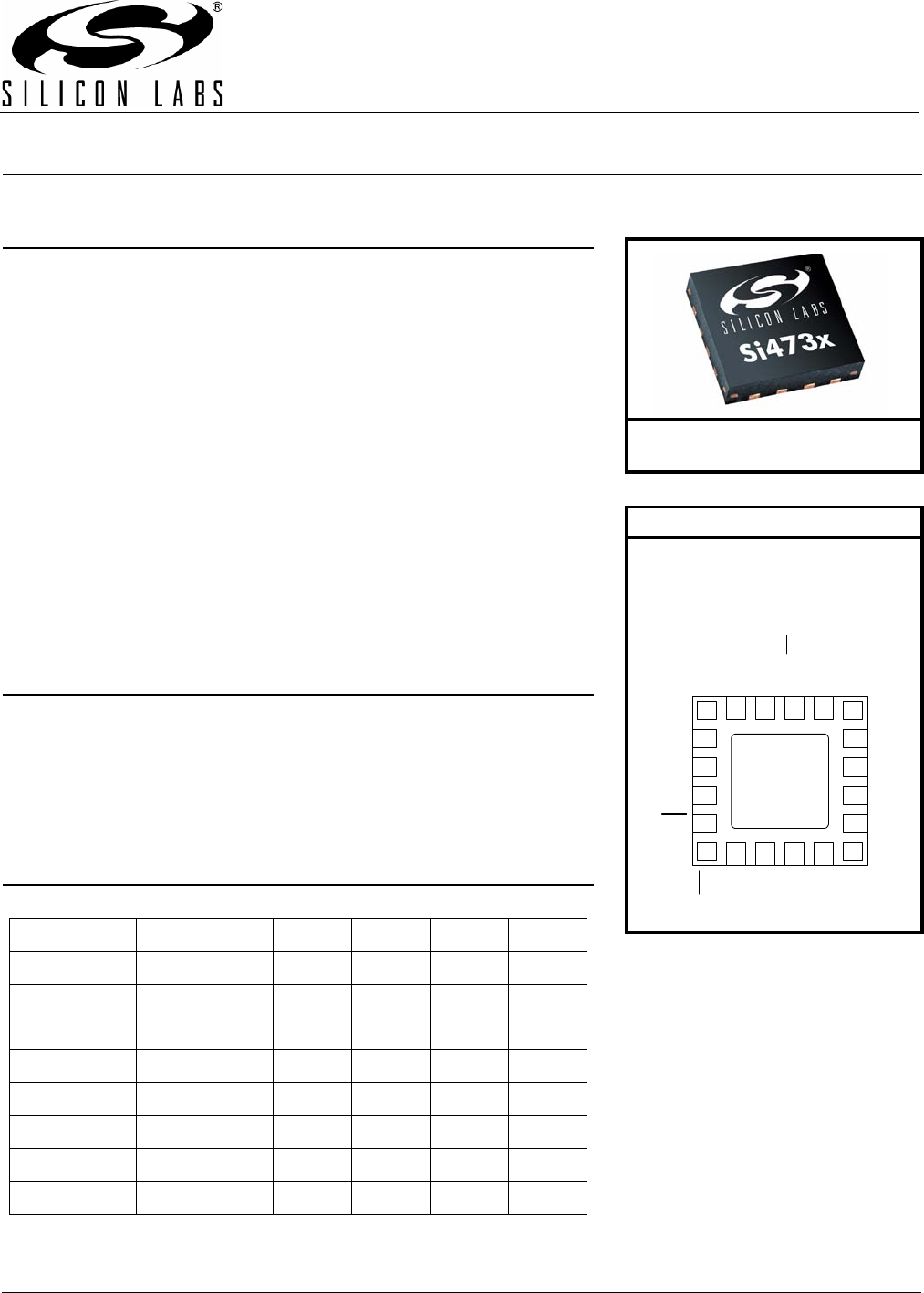
Si473x-B20Rev. 0.5 197. Package Outline: Si473x QFNFigure 5 illustrates the package details for the Si473x. Table 11 lists the values for the dimensi
Si473x-B202 Rev. 0.5
Si473x-B2020 Rev. 0.58. PCB Land Pattern: Si473x QFNFigure 6 illustrates the PCB land pattern details for the Si473x family. Table 12 lists the value
Si473x-B20Rev. 0.5 21Table 12. PCB Land Pattern DimensionsSymbol Millimeters Symbol MillimetersMin Max Min MaxD 2.71 REF GE 2.10 —D2 1.60 1.80 W — 0.3
Si473x-B2022 Rev. 0.59. Additional Reference ResourcesContact your local sales representatives for more information or to obtain copies of the follow
Si473x-B20Rev. 0.5 23NOTES:
Si473x-B2024 Rev. 0.5CONTACT INFORMATIONSilicon Laboratories Inc.400 West Cesar ChavezAustin, TX 78701Tel: 1+(512) 416-8500Fax: 1+(512) 416-9669Toll F
Si473x-B20Rev. 0.5 3TABLE OF CONTENTSSection Page1. Product Overview . . . . . . . . . . . . . . . . . . . . . . . . . . . . . . . . . . . . . . . . .
Si473x-B204 Rev. 0.51. Product OverviewThe Si473x receivers are the industry's first fully-integrated multiband radio receiver ICs from antenna
Si473x-B20Rev. 0.5 5Table 2. Absolute Maximum Ratings1,2Parameter Symbol Value UnitSupply Voltage VDD –0.5 to 5.8 VInterface Supply Voltage VIO–0.5 to
Si473x-B206 Rev. 0.5Table 3. DC Characteristics (VDD = 2.7 to 5.5 V, VIO = 1.5 to 3.6 V, TA = –20 to 85 °C)Parameter Symbol Test Condition Min Typ Max
Si473x-B20Rev. 0.5 7Figure 1. Reset Timing Parameters for Busmode SelectTable 4. Reset Timing Characteristics1,2(VDD= 2.7 to 5.5 V, VIO= 1.5 to 3.6 V
Si473x-B208 Rev. 0.5Table 5. 2-Wire Control Interface Characteristics1,2,3(VDD = 2.7 to 5.5 V, VIO = 1.5 to 3.6 V, TA = –20 to 85 °C)Parameter Symbol
Si473x-B20Rev. 0.5 9Figure 2. 2-Wire Control Interface Read and Write Timing ParametersFigure 3. 2-Wire Control Interface Read and Write Timing Diagra
More documents for Soundbar speakers American Audio B20

Related products and manuals for Soundbar speakers American Audio B20
 (16 pages)
 (16 pages)
© 2020, manymanuals.com. All rights reserved. | 1.646 s |
 Manymanuals.com
 Manymanuals.de
 Manymanuals.fr
 Manymanuals.it
 Manymanuals.pl
 Manymanuals.cz
 Manymanuals.es
 Manymanuals-pt.com
Comments to this Manuals